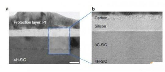
High resolution transmission electron microscopy showed that only after a 30 ns laser pulse, the silicon carbide (SiC) substrate melted and separated into a carbon layer and a silicon layer. More pulses lead to carbon layers organized into graphene, while silicon leaves in the form of gas.
All our smart phones have a sparkling AMOLED display. At least two of the silicon transistors are fabricated by laser pointer annealing at least of each pixel in the display screen. Conventional methods usually use temperatures above 1000 degrees C to create them, and laser technology can give the same results at low temperatures, even on plastic substrates (melting temperatures below 300 degrees C). Interestingly, similar processes can also be used to produce graphene crystals. Graphene is a kind of strong and thin nano material made of carbon, and its electrical conductivity and thermal conductivity have attracted the attention of scientists all over the world.
The Basic Science Research Institute (IBS) research group of Professor KEON Jae Lee multidimensional carbon materials center and South Korea Advanced Institute of science and Technology (KAIST) CHOI Sung professor Yool’s team found that the phase separation induced by laser single crystal silicon carbide (SiC) mechanism to synthesize graphene. The study, published in nature communications, describes how the laser technology can separate a complex compound (SIC) into carbon and silicon.
Although the basic research on some understanding of the effect of excimer green laser pointer in transformation of elemental materials such as silicon, but because of the complexity and processing time of compound phase change ultrashort laser, and more complex compounds such as the interaction between silicon carbide has rarely been studied.
By using the high resolution image and molecular dynamics simulation, the scientists found that xenon chloride excimer laser with a 30 nanosecond single pulse irradiation can melt SiC, which leads to the separation of liquid SiC layer, get on the surface of a disordered domain with a graphite carbon layer (2.5 nm thick) and a layer of carbon the polysilicon layer (5 nm). Additional pulses are applied to the separation of the silicon, and the disordered carbon layer is converted into a multilayer graphene.
“This study shows that laser and material interaction techniques can be a powerful tool for the next generation of two-dimensional nanomaterials,” said Professor Keon. Professor Choi added: “using 400mw laser pointer induced phase separation of complex compounds, a new type of two-dimensional materials can be synthesized in the future.” Keon professor IBS is affiliated with the KAIST Institute of materials science and engineering, and Professor Choi is part of the KAIST Institute of electrical engineering and graphene research center.
http://venturebeats.userecho.com/topics/966-application-of-laser-technology-in-mobile-phone/
http://laserman123456.kinja.com/industrial-applications-of-micro-lasers-1789677003
(12)
Tags: 400mw laser pointer, green laser pointer, laser pointer